DS1624
1 f 1
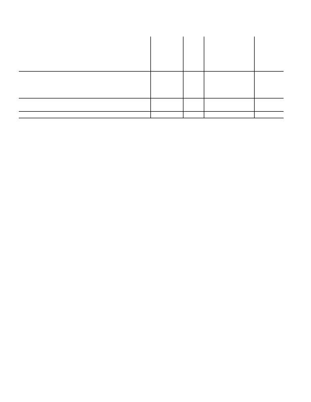
PARAMETER SYMBOL CONDITIONS
MIN
TYP MAX UNITS NOTES
Fall Time of Both
SDA and
SCL Signals
t
F
Fast mode
20+0.1C
B
300
ns
8, 9, 11
Standard mode
20+0.1C
B
300
Setup Time for
STOPCondition
t
SU:STO
Fast mode
0.6
祍
11
Standard mode
4.0
Capacitive Load for
Each Bus Line
C
B
400
pF
In ut Ca acitance
C
5
F
NOTES:
1. All voltages are referenced to ground.
2. I/O pins of fast mode devices must not obstruct the SDA and SCL lines if V
DD
is switched off.
3. I
CC
specified with SDA pin open.
4. I
CC
specified with V
CC
at 5.0V and SDA, SCL = 5.0V, 0?/SPAN>C to +70?/SPAN>C.
5. EEPROM inactive, temperature sensor in shutdown mode.
6. Write occurs between 0癈 and +70癈.
7. After this period, the first clock pulse is generated.
8. A fast mode device can be used in a standard mode system, but the requirement t
SU:DAT
e 250ns must
then be met. This is automatically the case if the device does not stretch the low period of the SCL
signal. If such a device does stretch the low period of the SCL signal, it must output the next data bit
to the SDA line t
R(MAX)
+t
SU:DAT
= 1000+250 = 1250ns before the SCL line is released.
9. For example, if C
B
= 300pF, then t
R(MIN)
= t
F(MIN)
= 50ns.
10. A master device must provide a hold time of at least 300ns for the SDA signal to bridge the undefined
region of SCLs falling edge.
11. See the timing diagram (Figure 2). All timing is referenced to 0.9V
DD
and 0.1V
DD
.
12. Limits are 100% production tested at T
A
= +25癈 and/or T
A
= +85癈. Limits over the operating
temperature range and relevant supply voltage are guaranteed by design and characterization.
发布紧急采购,3分钟左右您将得到回复。
相关PDF资料
DS1626S+
IC THERMOMETER/STAT DIG 8-SOIC
DS1629S+T&R
IC THERM/RTC/CALENDAR DIG 8-SOIC
DS1631S+T&R
IC THERMOMETER DIG HI-PREC 8SOIC
DS1721U+T&R
IC THERMOMETER/STAT DIG HP 8USOP
DS1722S
IC THERMOMETER DIG 3-WIRE 8-SOIC
DS1775R7+T&R
IC THERMOM/STAT DIG 111 SOT-23-5
DS1821C+
IC THERMOMETER/STAT PROG 3-TO92
DS1825U+T&R
IC THERMOMETER DIGITAL 8-USOP
相关代理商/技术参数
DS1625S
制造商:Maxim Integrated Products 功能描述:DIGITAL THERMOMETER, 8 Pin, SOP
DS1626
制造商:DALLAS 制造商全称:Dallas Semiconductor 功能描述:High-Precision 3-Wire Digital Thermometer and Thermostat
DS1626_07
制造商:DALLAS 制造商全称:Dallas Semiconductor 功能描述:High-Precision 3-Wire Digital Thermometer and Thermostat
DS1626S
功能描述:板上安装温度传感器 RoHS:否 制造商:Omron Electronics 输出类型:Digital 配置: 准确性:+/- 1.5 C, +/- 3 C 温度阈值: 数字输出 - 总线接口:2-Wire, I2C, SMBus 电源电压-最大:5.5 V 电源电压-最小:4.5 V 最大工作温度:+ 50 C 最小工作温度:0 C 关闭: 安装风格: 封装 / 箱体: 设备功能:Temperature and Humidity Sensor
DS1626S+
功能描述:板上安装温度传感器 Digital Thermometer & Thermostat RoHS:否 制造商:Omron Electronics 输出类型:Digital 配置: 准确性:+/- 1.5 C, +/- 3 C 温度阈值: 数字输出 - 总线接口:2-Wire, I2C, SMBus 电源电压-最大:5.5 V 电源电压-最小:4.5 V 最大工作温度:+ 50 C 最小工作温度:0 C 关闭: 安装风格: 封装 / 箱体: 设备功能:Temperature and Humidity Sensor
DS1626S+T&R
制造商:Maxim Integrated Products 功能描述:TEMP SENSOR DGTL 3-WIRE 8USOP - Tape and Reel 制造商:Maxim Integrated Products 功能描述:IC THERMOMETER/STAT DIG 8-SOIC
DS1626S+T&R
功能描述:板上安装温度传感器 Digital Thermometer & Thermostat RoHS:否 制造商:Omron Electronics 输出类型:Digital 配置: 准确性:+/- 1.5 C, +/- 3 C 温度阈值: 数字输出 - 总线接口:2-Wire, I2C, SMBus 电源电压-最大:5.5 V 电源电压-最小:4.5 V 最大工作温度:+ 50 C 最小工作温度:0 C 关闭: 安装风格: 封装 / 箱体: 设备功能:Temperature and Humidity Sensor
DS1626U
功能描述:板上安装温度传感器 RoHS:否 制造商:Omron Electronics 输出类型:Digital 配置: 准确性:+/- 1.5 C, +/- 3 C 温度阈值: 数字输出 - 总线接口:2-Wire, I2C, SMBus 电源电压-最大:5.5 V 电源电压-最小:4.5 V 最大工作温度:+ 50 C 最小工作温度:0 C 关闭: 安装风格: 封装 / 箱体: 设备功能:Temperature and Humidity Sensor
